Microchip design plays a critical role in the ever-evolving landscape of technology. As chip complexity continues to increase, so does the demand for advanced tools and methodologies to automate the design process. AI has made significant strides within the application layer for other domains like text, video, and audio. However, the application of LLMs specifically tailored for microchip design remains an untapped opportunity.
We’ll explore the gap & opportunity in the market for AI-powered microchip design and why I’m particularly excited to be funding companies bridging that gap.
Increasing complexity…
Microchip design is a highly intricate process involving complex layouts, intricate circuitry, and precise electrical characteristics. Traditionally, chip design has relied heavily on manual expertise, involving skilled engineers who spend a substantial amount of time and effort designing and optimizing these chips. Some see it as more of an ‘art than science’. Due to the nature of chip design, engineers often make decisions where there may not be a singular correct answer. It’s important to note that chip design is still heavily rooted in scientific principles and engineering methodologies. The manual approach often leads to multiple iterations, costly errors, and limited scalability.
The primary challenge we face heading into the future is the increasing complexity of chip architectures. As technology advances, chips become more densely packed with transistors, interconnects, and functional units. The efficiency of modern design tools needs to compliment the evolving nature of chip architecture. Chips are becoming more powerful and feature-rich, therefore they tend to consume higher amounts of power. Engineers will have to manage power dissipation, heat generation, and thermal hotspots. Certain techniques like voltage scaling, clock gating, and power gating, will need to be employed in order to optimize power consumption without compromising performance.
The time-to-market pressure in the semiconductor sector poses a significant challenge for chip designers. As history has shown us, technological advancements demand rapid deployment cycles and quick product launches. Design teams are faced with tight deadlines while all at the same time racing to meet performance targets, power constraints, and reliability requirements. The need for efficient software and tools has become paramount.
Market Opportunity
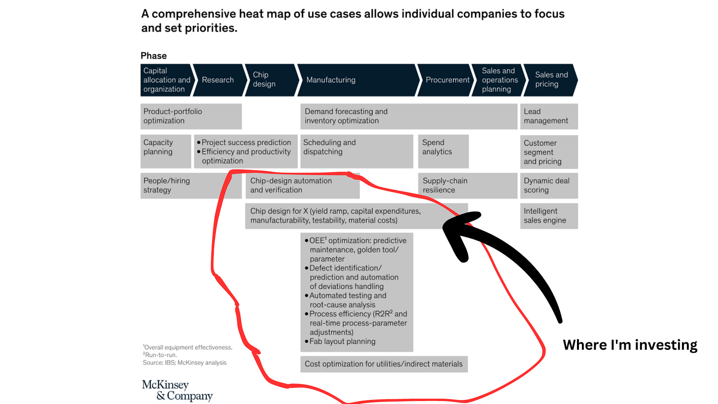
The market for microchip design is huge, driven by the relentless demand for innovative tech across industries. According to McKinsey and Company, AI/ML contributes between $5 billion and $8 billion annually to earnings before interest and taxes at semiconductor companies. The global semiconductor market is projected to reach $1.2 Trillion by the end of the decade.
Chip Floor planning (Graph Placement)
Floor planning or layout engineering is a functional step in microchip design that involves determining the optimal placement of functional blocks and components on a chip’s silicon area. It’s a crucial task that lays the foundation for subsequent steps in the design flow, such as routing and physical implementation.
The goal is to allocate the available chip area efficiently, considering various design objectives and constraints (like mentioned above).
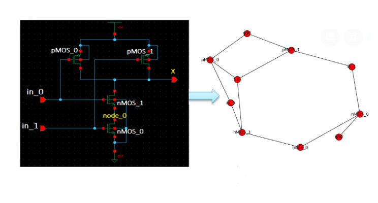
Graph Theory is a branch of mathematics and computer science that deals with the study of graphs, which are mathematical structures consisting of nodes and edges that connect pairs of nodes. Nodes represent entities, while edges represent the relationship of connection between these entities. Graph Theory provides a framework for analyzing and solving problems in relation to connectivity, paths, cycles, flows, and other properties of graphs.
Floor planning can be viewed as a graph placement problem, where functional blocks and components are represented as nodes, and the connections between them are represented as edges. The objective is to find an optimal arrangement of the nodes that minimizes the total wire-length and satisfies other constraints. Routing algorithms determine the most efficient paths for electrical signals to traverse the chip, while layout optimization algorithms help in arranging the components on the chips’s surface to minimize signal delays and improve performance. During the layout process, the designer considers various factors, such as the size and shape of the components, the connectivity requirements, and the available chip area.
To address these challenges, automated floor planning methods have been developed. These methods leverage algorithms to explore the design space more efficiently. An example of this is Reinforcement learning.
Reinforcement Learning
Reinforcement Learning (RL) is an area of machine learning that has gained attention in the recent years for its potential applications in various domains. It focuses on an artificial agent interacting with an environment, learning to make decisions and take actions that maximize a cumulative reward signal.
In the game of chess, reinforcement learning has been utilized to train agents capable of playing at a high level. Through self-play and exploration, RL agents learn to make decisions that maximize their chances of winning. They analyze game states, evaluate potential moves, and learn from the outcomes of different actions. Deep RL algorithms, such as AlphaZero, have achieved outstanding results, even surpassing human performance. RL has shown even more impressive results with the game of Go. AlphaGo, an RL-based system developed by DeepMind, has defeated world champion players.
As for chip design, RL can be employed to optimize component placement, routing, power optimization, and performance enhancement. RL offers a potential solution by using trial-and-error exploration to learn an optimal component placement strategy. Through iterative interactions with the chip design environment, RL agents can learn from previous designs and gradually improve their placement policies. The agents will consider multiple factors such as wire-length, reducing power consumption, improving signal integrity, and reducing thermal hotspots, simultaneously optimizing the chip’s overall performance.
The complexity and states in chip placement differ from games like chess and Go. While games involve discrete states and finite action spaces, chip placement involves continuous variables, such as physical positions and orientations of components. Training RL agents requires the production of larger scale datasets and appropriate simulation environments. Generating diverse datasets of chip designs and their corresponding performance metrics can be resource-intensive. The number of possible chip configurations is vast making it harder to explore the entire space within reasonable timeframes.
Despite the complexity, I’m very much optimistic about where we’re heading and the potential for AI to deliver exceptional results.
Does Nvidia Need AI More Than AI Needs Nvidia?
I won’t go too deep into this theory but I will say that the pace at which we are going with the development and application of AI, something needs to happen here.
The release of GPT-3 & 4 has not only been disruptive in terms of the application of AI but it has also set of an arms race for creating stronger and faster models. While GPUs are primarily designed for accelerating graphics rendering, their parallel processing capabilities make them highly efficient for various computationally intensive tasks, including NLP. By replacing CPUs with GPUs, AI algorithms can be trained at a much faster pace.
ChatGPT itself was trained using 10,000 NVIDIA GPUs. 😲
NVIDIA, the most prominent player in the semiconductor industry, has been the de-facto GPU server for most AI solutions. Last month, we saw NVIDIA’s stock briefly kiss the $1 Trillion market cap and for us spectators it feels like it came out of nowhere. It has only propelled the belief that they will be the true winners in the AI gold rush.
GPU shortage is no joke. Demand is rising and will continue to rise as AI eats the world. NVIDIA has an opportunity to enhance the chip production process by employing AI agents and deep learning techniques. They can optimize various stages of chip manufacturing, from design to production. In addition, AI can analyze vast amounts of manufacturing data, enabling real-time observability, predictive maintenance, and quality control. NVIDIA could potentially identify and address issues early on, thus enhancing yield and expediting the entire manufacturing process.
Let the chips fall where they may..
I believe that the application of AI/ML will inherently accelerate the semiconductor industry over the next decade. This is where we will see the most value accrued from the advancements in AI/ML. If you’re building ANYTHING that falls into this bucket, feel free to reach out! I’m curious to learn more! :)


What a thoughtful and well written piece!
AI has massive opportunities to help radically improve the design process for semiconductors. Many of the Integrated Circuit designers are looking for new tools to improve design productivity and simulation time with AI.
One question though is why you believe LLMs can be applied to Chip design? Is this the idea that designers can use natural language to set chip parameters rather than HDL?